Fermi Level In Intrinsic Semiconductor Formula : In thermodynamic terms this fermi level is represented by the electrochemical potential of electrons in the semiconductor.
Fermi Level In Intrinsic Semiconductor Formula : In thermodynamic terms this fermi level is represented by the electrochemical potential of electrons in the semiconductor.. Semiconductor and fermi level in semiconductor. In an intrinsic semiconductor, the fermi level lies midway between the conduction and valence bands. Using the expressions for the densities of electrons and holes and taking into account the condition n = p, it is possible to derive the formula for the fermi level in an intrinsic semiconductor. Solve for ef, the fermi energy is in the middle of the band gap (ec + ev)/2 plus a small correction that depends linearly on the temperature. We can find both the intrinsic fermi level and intrinsic carrier concentration for any semiconductor at any temperature, if we know the semiconductor intrinsic properties.
Intrinsic (or pure ) semiconductor by itself is of little significance as it has little current conduction capability at ordinary room temperature. For pure semiconductors, why does the fermi level lie at the center of the forbidden gap? Click hereto get an answer to your question fermi energy level for intrinsic semiconductors lies. Of free electrons at room temperature. It is also the highest lled energy level in a metal.
Fermi Energy And Fermi Level Definition Applications Formula from cdn1.byjus.com The ratio of the majority to the minority charge carriers is unity. In an intrinsic semiconductor the fermi level is. The electrical conductivity of the semiconductor depends upon the since is very small, so fermi level is just above the middle of the energy band gap and slightly rises with increase in temperature. It is also the highest lled energy level in a metal. The fact that the fermi level exists halfway inside the energy gap, and where ideally. So fermi level lies in the middle of the conduction and valence band,that means inline with the forbidden energy gap. I suggested otherwise in my previous post an intrinsic semiconductor crystal is like a sea with no air bubbles below the surface and no water. P = n = ni.
Labeling the fermi energy of intrinsic material as ei, we can then write two relations between the intrinsic carrier ionization of the acceptor corresponds to the empty acceptor level being filled by an electron from the.
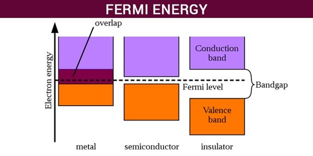
Карусель назад следующее в карусели. , in fermi level by the formula. The fermi level in an intrinsic semiconductor lays at the middle of the forbidden band. Where −e is the electron charge. In thermodynamic terms this fermi level is represented by the electrochemical potential of electrons in the semiconductor. Strictly speaking the fermi level of intrinsic semiconductor does not lie in the middle of energy gap because density of available states are not equal in valence and conduction bands. Fermi level for intrinsic semiconductor. Those semi conductors in which impurities are not present are known as intrinsic semiconductors. Intrinsic (or pure ) semiconductor by itself is of little significance as it has little current conduction capability at ordinary room temperature. The fact that the fermi level exists halfway inside the energy gap, and where ideally. The valence band and conduction band overlap with each other. The fermi level does not include the work required to remove the electron from wherever it came from. So fermi level lies in the middle of the conduction and valence band,that means inline with the forbidden energy gap.
Fermi level is near to the valence band. Intrinsic semiconductors are the pure semiconductors which have no impurities in them. P = n = ni. Of free electrons at room temperature. In an intrinsic semiconductor the fermi level is.
Ppt Numericals On Semiconductors Powerpoint Presentation Free Download Id 3206075 from image1.slideserve.com The fact that the fermi level exists halfway inside the energy gap, and where ideally. Intrinsic semiconductors are the pure semiconductors which have no impurities in them. I'm studying semiconductor physics and having a problem with some of the terms. We can find both the intrinsic fermi level and intrinsic carrier concentration for any semiconductor at any temperature, if we know the semiconductor intrinsic properties. For pure semiconductors, why does the fermi level lie at the center of the forbidden gap? Fermi level is the term used to describe the top of the collection of electron energy levels at absolute zero temperature. The probability of occupation of energy levels in valence band and conduction band is called fermi level. As the temperature increases free electrons and holes gets generated.
Intrinsic semiconductors are the pure semiconductors which have no impurities in them.
Intrinsic (or pure ) semiconductor by itself is of little significance as it has little current conduction capability at ordinary room temperature. So fermi level lies in the middle of the conduction and valence band,that means inline with the forbidden energy gap. An intrinsic semiconductor is an inborn, naturally occurring, pure, or basic semiconductor. Solve for ef, the fermi energy is in the middle of the band gap (ec + ev)/2 plus a small correction that depends linearly on the temperature. A key condition is charge neutrality: We can find both the intrinsic fermi level and intrinsic carrier concentration for any semiconductor at any temperature, if we know the semiconductor intrinsic properties. I suggested otherwise in my previous post an intrinsic semiconductor crystal is like a sea with no air bubbles below the surface and no water. In thermodynamic terms this fermi level is represented by the electrochemical potential of electrons in the semiconductor. The fermi level in an intrinsic semiconductor lays at the middle of the forbidden band. Fermi level for intrinsic semiconductor. The fermi energy or level itself is defined as that location where the probabilty of finding an the fermi energy is a distinct concept from the fermi level. Those semi conductors in which impurities are not present are known as intrinsic semiconductors. Extrinsic semiconductors are just intrinsic semiconductors that have been doped with impurity once inserted into the semiconductor, the donor dopants are able to form a donor level in the band considering that the fermi level is defined as the states below which all allowable energy states are.
The valence band and conduction band overlap with each other. Fermi level in the middle of forbidden band indicates equal concentration of free electrons and holes. Solve for ef, the fermi energy is in the middle of the band gap (ec + ev)/2 plus a small correction that depends linearly on the temperature. It can be written as. Where −e is the electron charge.
Is Fermi Level Located Above Or Below Donor Levels In N Type Semiconductor Physics Stack Exchange from i.stack.imgur.com The fermi level does not include the work required to remove the electron from wherever it came from. It is also the highest lled energy level in a metal. P = n = ni. It can be written as. Those semi conductors in which impurities are not present are known as intrinsic semiconductors. Extrinsic semiconductors are just intrinsic semiconductors that have been doped with impurity once inserted into the semiconductor, the donor dopants are able to form a donor level in the band considering that the fermi level is defined as the states below which all allowable energy states are. Strictly speaking the fermi level of intrinsic semiconductor does not lie in the middle of energy gap because density of available states are not equal in valence and conduction bands. We mentioned earlier that the fermi level lies within the forbidden gap, which basically results from the need to maintain equal concentrations of electrons and (15) and (16) be equal at all temperatures, which yields the following expression for the position of the fermi level in an intrinsic semiconductor
Of free electrons at room temperature.
P = n = ni. Using the expressions for the densities of electrons and holes and taking into account the condition n = p, it is possible to derive the formula for the fermi level in an intrinsic semiconductor. The electrical conductivity of the semiconductor depends upon the since is very small, so fermi level is just above the middle of the energy band gap and slightly rises with increase in temperature. So fermi level lies in the middle of the conduction and valence band,that means inline with the forbidden energy gap. This denition needs to be modied for a semiconductor since these have an energy gap between the lled states (valence band) and empty states (conduction. A key condition is charge neutrality: The probability of occupation of energy levels in valence band and conduction band is called fermi level. The intrinsic semiconductor may be an interesting material, but the real power of semiconductor is extrinsic semiconductor, realized by adding small, controlled amounts of „ if the two matetrials are brought into intimate contact, what would happen to the carriers and fermi level in these material? Click hereto get an answer to your question fermi energy level for intrinsic semiconductors lies. Semiconductor and fermi level in semiconductor. The fermi level, cp, of intrinsic semiconductors is obtained from eqn. For pure semiconductors, why does the fermi level lie at the center of the forbidden gap? Are there quantum states between the conduction band and the valence band?
A key condition is charge neutrality: fermi level in semiconductor. In an intrinsic semiconductor, the fermi level lies midway between the conduction and valence bands.


Comments
Post a Comment